Pn Junction Diode Forward Bias Circuit Diagram Diode Junctio
Pn junction diode (forward-bias condition), 58% off What is a junction diode? what are the types of junction diodes Schematic diagram of forward biased diode
Forward biasing of p-N junction diode - YouTube
Pn junction diode: forward and reverse bias characteristics Pn junction diode and its forward bias & reverse bias characteristics ☑ diode zero bias
Diode biased pn biasing bias definition electricalworkbook
What is forward bias and reverse bias? example, applicationsPn junction under reverse bias condition Bias diode forward pn junction currentDiode forward junction bias types pn working electrical4u reverse biased diodes principle current diffusion under type symbol semiconductor electrons depletion.
Junction bias pn appliedDiode junction pn bias forward characteristics depletion voltage electronics current region circuits mosfet bjt formation biased reverse semiconductors under ws Forward bias and reverse bias of pn junction diodeBias pn junction diode.

Bias reverse forward diode electronics
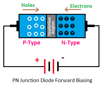
Pn junction forward bias circuit diagramForward biasing of pn junction diode Biasing difference bias diode voltageForward biased p-n junction diode.
Pn junction circuit diagram zero biasMiirbe pn junction diode forward bias diagram Difference between forward & reverse biasing with comparison chartForward and reverse bias circuit diagram.

To draw the i-v characteristic curve of a p-n junction in forward bias
An introduction to p-n junction diode and its workingP-n junction Electrical – how to discharge the pn junction capacitance – valuableSemiconductor diode.
Pn junction diode animation pptDiode pn semiconductor junction layer depletion working bias reverse characteristics notes physics flow circuit electronics biasing type battery choose board Junction forward region depletion diagram pn biased showing including figureForward and reverse bias of a pn junction (explained).

Diode pn zener bias chart ppt
Junction diode forward biasing working bias pn its reverse voltage introductionDiodo a giunzione pn e caratteristiche del diodo Diode junction pn forward bias characteristics circuit biasing reverse ammeter voltmeter plot sourcePn junction diode forward and reverse bias.
Pn junction diode forward bias current part 1Junction bias draw arrangement studying pn diode reverse plot reversed obtaining ☑ diode zero biasDiode action.

Forward junction diode biasing
Forward diode junction biased hole current semiconductor electron diodes bias holes voltage appliedPn junction diode Semiconductor diodeDraw the circuit arrangement for studying v-i characteristics of a p-n.
Diode forward bias circuit diagramReverse biasing of pn junction diode Bias biasing pn diode junction etechnog transistors barrierForward biasing of p-n junction diode.


Pn Junction Circuit Diagram Zero Bias

Diodo a giunzione PN e caratteristiche del diodo | Arquidia Mantina

☑ Diode Zero Bias

PN Junction Diode and its Forward bias & Reverse bias characteristics
What is Forward Bias and Reverse Bias? Example, Applications - ETechnoG

Forward biasing of p-N junction diode - YouTube

pn junction under reverse bias condition